- Number of Layers
- PCB Dimensions
- PCB Shape
- Internal Cutouts
- Slits (Internal Cutouts)
- Minimum Pattern Width
- "Minimum Clearance (Insulation Distance)"
- Minimum Distance Between Lands (Pads)
- Minimum Annular Ring Thickness
- Minimum Distance from PTH Edge to Copper Foil
- Minimum Distance from PCB Edge to Copper Foil
- BGA Patterns
- Solid Pattern (Copper Plane)
- Solder Resist (Solder Mask)
- Minimum Solder Resist Width
- Minimum Solder Resist Clearance
- Solder Resist Restricted Areas
- Distance from Solder Resist Opening to Adjacent Pattern
- General Solder Resist Guidelines
- Drilling (Holes)
- Minimum Hole Diameter
- Maximum Hole Diameter
- Plated Through-Holes
- Non-Plated Through-Holes
- Long Holes
- Square Holes
- Edge Plated Through-Holes
- Minimum Distance from PCB Edge to Hole Edge
- Minimum Distance Between Hole Edges
- Silkscreen Printing
- Minimum Silkscreen Width
- Minimum Silkscreen Clearance
- Silkscreen Restricted Areas
- V-Cut
- PCB Data
- Manufacturing Standards
- Base Material
- PCB Thickness
- Tolerance for PCB Thickness
- External Dimension Tolerance
- Outer Shape Processing
- Warpage
- V-CUT
- Copper Foil Purity
- Copper Foil Thickness
- Copper Plating Thickness
- Surface Finish for Lands (Pads)
- Solder Resist(Solder Mask) Color
- Solder Resist(Solder Mask) Thickness
- Drilling (Holes)
- Copper Plating Thickness for Through-Holes
- Silkscreen Printing Color
- Our Printed Information (printed characters)
- Manufacturing Facility
Number of Layers
1~20
Up to 20 layers available.
PCB Dimensions
Minimum: 10mm × 10mm.
Maximum: 500mm × 500mm.
Minimum order area is 0.0001㎡.
PCB Shape
Rectangle and square are [standard] and other shapes
The figure below is an example of other shapes.
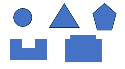
*When installing protrusions on custom shapes, we recommend that the width of the protrusions be 3 mm or wider.
Protrusions thinner than that may cause cracking.
Internal Cutouts
A slit is designed on the PCB. Or a circle with a diameter of 6 mm or more is designed on the PCB.
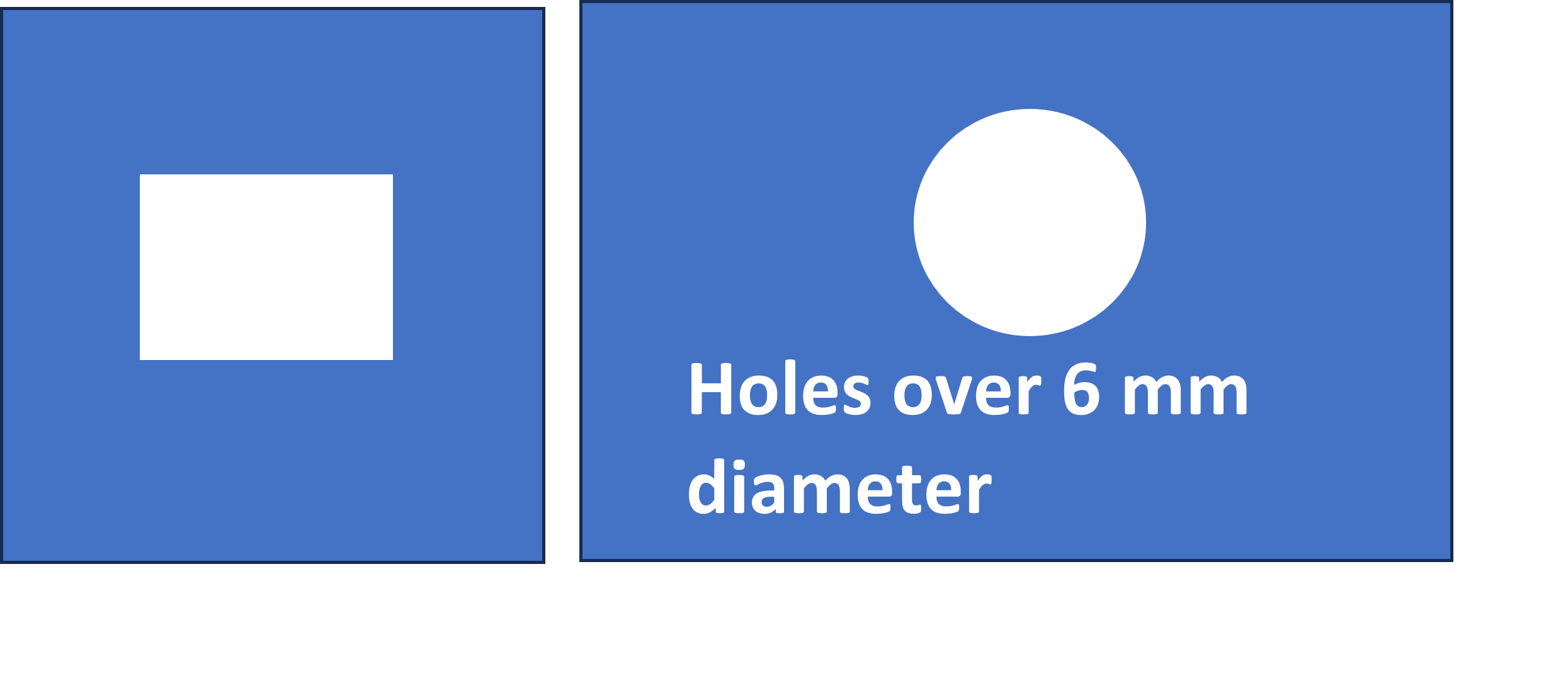
*Since cutting is performed with a rotary blade of 2.0 mm or 1.0 mm in diameter, a rounded curve will result when hollowing out at a right angle, for example.
Especially when imposition is made, design the external shape (router track) taking into account the 2mm diameter of the blade. As for the cutout of the discarded board part, adjust the cutout shape at the factory accordingly.
*If internal cutouts are made on areas with copper foil, they may result in through holes (hole wall plating).
To ensure non through-hole, remove 0.3mm of copper foil around the cutout.
Slits (Internal Cutouts)
Standard width: 2.0mm or more.
Minimum width: 1.0mm.
Additional charges may apply for widths below 2.0mm.
Minimum Pattern Width
0.125mm(Copper foil thickness 35um)【standard】
0.10mm(Copper foil thickness18um)
0.18mm(Copper foil thickness70um)
0.20mm(Copper foil thickness105um)
0.076mm(Copper foil thickness18um)【option】
Minimum Clearance(Insulation Distance)
0.125mm(Copper foil thickness 35um)【standard】
0.10mm(Copper foil thickness18um)
0.18mm(Copper foil thickness70um)
0.20mm(Copper foil thickness105um)
0.076mm(Copper foil thickness18um)【option】
Minimum Distance Between Lands (Pads)
0.125mm(Copper foil thickness 35um)【standard】
0.10mm(Copper foil thickness18um)
0.18mm(Copper foil thickness70um)
0.20mm(Copper foil thickness105um)
0.076mm(Copper foil thickness18um)【option】
Minimum Annular Ring Thickness
Standard: 0.20mm or more.
<Exceptions
1, For VIA with a hole diameter of 0.3 mm or less: Annular ring thickness of 0.10 mm or more
(However, this is limited to cases where the copper foil thickness is 35um or less)
(e.g., for VIA with a hole diameter of 0.3mm, a pad diameter of 0.5mm or larger is required)
However, the finished hole diameter may be smaller than the designed value.
*If there is room in the pattern, 0.2mm or more is recommended.
2,Non-through holes on single-sided boards: Annular ring thickness of 0.10 mm or more
(e.g., for a non through-hole with a hole diameter of 0.7mm, a pad diameter of 0.9mm or more is required)
*If there is room in the pattern, 0.2mm or more is recommended.
3,Inner layer annular ring thickness 0.10mm or more
(e.g., for VIA with a hole diameter of 0.3mm, an inner layer pad diameter of 0.5mm or more is required)
*If there is room in the pattern, 0.2mm or more is recommended.
4,End-face through-hole: Annular ring thickness of 0.50mm or more
Minimum Distance from PTH Edge to Copper Foil
0.2mm (for inner layers or vias without annular rings).
Minimum Distance from PCB Edge to Copper Foil
0.5mm.
BGA Patterns
For pads with diameters of 0.4mm or less, copper foil thickness of 18um is recommended.
Solid Pattern (Copper Plane)Keep sufficient clearance between copper planes and adjacent patterns. Ensure balanced copper distribution on both sides of the PCB to prevent warping. Mesh patterns should have a line width of 0.25mm or more and a spacing of 0.25mm or more.
Solder Resist (Solder Mask)
Double-sided [Standard for 2L],
Single-sided [Standard for 1L]
No Solder Mask
Minimum Solder Resist Width
Resist green copper foil 35um or less ・・・ 0.1mm
Resist green, copper foil 70um or more ・・・ 0.15mm
Resist other than green, copper foil 35um or less ・・・ 0.15mm
Resist other than green, copper foil 70um or more ・・・ 0.20mm
Minimum Solder Resist Clearance
Resist green copper foil 35um or less ・・・ 0.1mm
Resist green, copper foil 70um or more ・・・ 0.15mm
Resist other than green, copper foil 35um or less ・・・ 0.15mm
Resist other than green, copper foil 70um or more ・・・ 0.20mm
Solder Resist Restricted Areas
Resist openings of 0.05mm or more around through holes/non-through holes should be resist openings.
(Hole diameter + resist opening of 0.1mm or more)
However, for VIA, resist openings are not required only when there is no problem even if the holes are filled with resist.
Distance from Solder Resist Opening to Adjacent Pattern
At least 0.1mm.
General Solder Resist Guidelines
To account for resist printing misalignment, etc., the resist aperture is indicated slightly larger than the land size.
Typical values are shown below.
(Example 1) In the case of land size φ1.0, resist aperture is φ1.1
(with a margin of 0.05mm on one side)
(Example 1) In the case of land size φ1.0, resist aperture is φ1.1
(with a margin of 0.05mm on each side)
In the following cases, resist size may be adjusted by editing data before manufacturing.
(1) When the resist aperture size is small and there is a possibility that the resist will cover the land.
(2) When the resist aperture size is large and there is a possibility of exposing the surrounding patterns or solid conductors.
Drilling (Holes)
Hole diameter should be indicated by the finished size (diameter).
The finished size refers to the hole diameter before solder leveling.
Please take into consideration that the hole diameter will be reduced by the solder leveler.
Minimum Hole Diameter0.25mm [standard],
0.15mm (through hole) [option],
0.1mm (non through hole) [option].
However, the thickness is limited to the board thickness with an aspect ratio of 8:1.
Maximum Hole Diameter6.0mm
Holes larger than 6.0mm will be router cut.
Plated Through-Holes
Holes on a multilayer board are basically through holes.
Through holes should have lands (pads) and annular rings on both sides.
If there are lands on only one side, it will be a non-through hole in most cases.
(It is not guaranteed to be either a through hole or a non through hole due to factors such as hole diameter, board thickness, and manufacturing variations.)
<Caution
Even if the instruction for Through Hole or Non-Through Hole is given in the drill data or report file, it will be ignored.
Through-holes and non-through holes are automatically determined by the presence or absence of lands.
Non-Plated Through-HolesWhen non through-holes (holes without plating) are made on boards with two or more layers, copper foil cannot be placed 0.30 mm around the holes.
(Basically, it is recommended that all component lands be through-holes.)
Long Holes
The short side must be 0.5mm or more,
and the long side must be at least twice the short side.
Square Holes
Not possible due to drill processing. Use longholes instead.
Edge Plated Through-Holes
Plated half through-holes can be processed.
(Additional cost will be incurred due to special processing.)
Please place a through-hole (land required) on the outline line where the plated half through-holes is to be made.
It is also possible to form end-face through holes with long holes.
Minimum Distance from PCB Edge to Hole Edge
1.5mm (0.5mm if cracks or chips are acceptable).
Minimum Distance Between Hole Edges
0.20mm.
Silkscreen Printing
Printing on one side (standard), both sides, or no printing.
Minimum Silkscreen Width
0.127mm or more (recommended: 0.2mm).
Minimum Silkscreen Clearance
0.127mm or more.
Silkscreen Restricted Areas
Do not print within 0.05mm of solder mask openings,
Basically, the above range is silk-cut (silk-removed) in the data editing process before manufacturing.
However, silk cutting may not be performed if the resist aperture size is large, etc. If silk printing is desired, please delete silk printing at the design stage.
Silk printing is prohibited in 0.2mm around non through holes and through holes.
(Because there is a possibility that ink may flow into the drill holes.)
In addition, 0.3mm from the edge of the board and 0.3mm from the land (pad) may not be printed.
Especially when silk printing within 0.1mm around land (pad), there is a possibility that ink may be placed on the land due to silk printing misalignment or blotting of silk ink. When silk-printing around the land, please allow for the above risks.
V-Cut
V-cut can be processed on substrates with a thickness of 0.6 mm to 2.0 mm.
However, for thicknesses of 1.0 mm or less, the depth of the V-cut groove may vary.
V-cut instructions are drawn in the outline data, and “←V-CUT” is used for V-cut.
If V-CUT” cannot be inserted due to CAD limitations or other reasons, it can be omitted.
If V-cut cannot be drawn in the outline data, it is acceptable to use independent V-cut data (Gerber file).
V-cut must always cut through the board outline. Jump V-cuts are not allowed.
The V-cut must be parallel to the X-axis or Y-axis of the board.
The V-cut dividing line must be drawn with a thickness of about 0.5 mm.
(The V-cut blade width is constant, so changing the drawing thickness will not be reflected in the actual processing.)
Please use long holes or perforations in conjunction with the “wrong example” method of imposition.
Perforation imposition does not cause a dedicated layer, but draws in holes or long holes on a conventional drill layer.
PCB Data
All data should be in transparency view of the part surface (first layer surface view).
Gerber format should be Extended Gerber (RS-274X) or Gerber X2.
Exelon (NC) format is recommended for drill files. In this case, the drill hole diameter information should be embedded in the coordinate file as much as possible.
Please rename the Gerber data for each layer to the following file names or create a table of file name and layer correspondence.
(You do not need to attach files for unnecessary layers.)
ptn_top.grb: Part surface (layer 1) copper foil pattern
ptn_sec.grb: Copper foil pattern on layer 2 (inner layer)
ptn_thi.grb: Copper foil pattern on layer 3 (inner layer)
ptn_fou.grb: Layer 4 (inner layer) copper foil pattern
ptn_fiv.grb: Layer 5 (inner layer) copper foil pattern
ptn_btm.grb: Copper foil pattern on solder surface
res_top.grb: Resist on component surface
Res_btm.grb: Resist on solder side
slk_top.grb :Silk print on component surface
slk_btm.grb :Silk print on solder side
Outline.grb: PCB outline
dri.grb : Drill file (Through hole and Non-through hole can be mixed)
NPTH.grb : Drill file (Non-through holes on boards with two or more layers)
*Only when output is separated from through holes
However, if there is any inconvenience in management, etc., there is no problem even if the extension is changed to “.grb”.
<Recommended and deprecated settings for Gerber data
360-degree arcs (circular arcs) are not recommended.
It is recommended to draw arcs of 180 degrees by connecting them.
When using a 360-degree arc, be sure to embed the G75 command in the Gerber data.
(Instructions in the report file are not acceptable.)
Polygons are not recommended.
It is recommended to use line fill.
Manufacturing Standards
Standards for materials, dimensions, and tolerances.
Base Material
FR-4 (glass epoxy copper-clad laminate).
If you would like to use other materials (CEM-3, FR-1, etc.), please contact us by e-mail.
PCB Thickness
1.6mm [standard]
1mm
1.2mm
2mm
*The following plate thicknesses can also be manufactured. Please inquire by e-mail.
0.2mm (single or double-sided substrate),
0.4mm (single or double-sided substrate),
0.6mm (single or double-sided substrate),
0.8mm,
2.4mm,
3.2mm,
4mm,
5mm,
6mm
Tolerance for PCB Thickness
±10% (or ±0.1mm for boards thinner than 1mm)
External Dimension Tolerance
±0.3mm (±0.6mm if no reference hole is present).
Outer Shape Processing
Since the board exterior is cut out with a router, the corners of the recesses will be rounded.
The same is true when drilling square holes inside the board.
The trajectory of the router is determined by looking at the placement of the surrounding patterns, etc. (It either bites inside or goes through the outside.)
If you have a specification for the orbit of the router, please specify the finished shape with R1.5 on the corners at the Gerber data creation stage.
Warpage
The warpage of a substrate shall be less than 1.5% of its length in the longitudinal direction or 1 mm, whichever is greater.
However, the following substrates are excluded.
Substrates with a thickness of less than 1.6 mm
Boards with V-cuts or router cutouts
Substrate with a large difference in the percentage of copper foil remaining on the component and solder surfaces.
When there is a partial solid surface.
When the length-to-breadth ratio of the board size is longer than 1:3.
Other cases where warpage is likely to occur due to design
V-CUT
V-cut width: approx. 0.5 mm (on a board 1.6 mm thick)
A positioning hole (about 0.5 mm dia.) may be drilled near the beginning and end of the V-cut.
Copper Foil Purity
99.5% or higher.
Copper Foil Thickness
Outer layers: 35um (standard), 18um・70um・105um・140um・175um・210um・245um・280um・315um・350um
Inner layers: 35um (standard), 18um・70um・105um・140um
Copper Plating Thickness
10–20um.
Surface Finish for Lands (Pads)
HASL (standard), ENIG, Lead-Free HASL, Preflux(OSP), Electrolytic plating and hard gold.
*Quality Standards
No copper plating shall be exposed on the land area.
Chipping of copper foil should be limited to 2/5 of the pattern width.
Solder Resist(Solder Mask) Color
Green (standard), blue, black, red, white, yellow. Solder Resist(Solder Mask) ThicknessApproximately 16um.
*Quality Standards
No exposed copper plating on lands. Pattern chipping up to 2/5 of the width is allowed. Solder resist misalignment: ±0.1mm.
Drilling (Holes)
All single-sided boards will be non-through holes.
For boards with two or more layers, through holes (holes with plating) are basically used.
However, holes without lands (annular rings) on both sides are non-through holes.
Holes with lands on only one side for boards with 2 or more layers are not guaranteed to be either through holes or non through holes, so please design them to avoid this as much as possible.
For boards with 4 or more layers, please be sure to provide lands on the surface layer (both on the component side and the solder side) for holes that you want to use as through holes.
For example, VIA that passes signals from L2 to L3 on a 4-layer board also requires lands (annular rings) on L1 and L4.
Hole diameter tolerance: ±0.075mm (through-hole), ±0.05mm (non through-hole)
Hole diameter tolerance is fixed at the above values.
Tolerances specified in drill data, report files, hole drawings, drill maps, etc. are not reflected in manufacturing.
Please adjust the center value of the hole diameter (aim value) according to the above tolerance.
Copper Plating Thickness for Through-Holes
10–20um.
Silkscreen Printing Color
White (standard), black, yellow.
Our Printed Information(printed characters)
UL marks, manufacturing control numbers, lots, etc. may be printed.
Manufacturing
FacilityProducts are manufactured in UL certified facilitys in China, Korea, or Japan.